- 您现在的位置:买卖IC网 > Sheet目录317 > CAT24C03WI-G (ON Semiconductor)IC EEPROM SERIAL 2KB I2C 8SOIC
�� �
�
�CAT24C03,� CAT24C05�
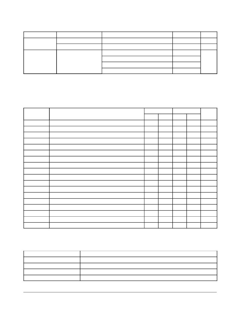
�Table� 4.� PIN� IMPEDANCE� CHARACTERISTICS�
�(V� CC� = 1.8 V to 5.5 V, T� A� =� ?� 40� °� C� to� +85� °� C,� unless� otherwise� specified.)�
�Symbol�
�C� IN� (Note� 4)�
�I� WP� (Note� 5)�
�Parameter�
�SDA� I/O� Pin� Capacitance�
�Input� Capacitance� (Other� Pins)�
�WP� Input� Current�
�Conditions�
�V� IN� =� 0� V�
�V� IN� =� 0� V�
�V� IN� <� V� IH� ,� V� CC� =� 5.5� V�
�Max�
�8�
�6�
�200�
�Units�
�pF�
�pF�
�m� A�
�V� IN� <� V� IH� ,� V� CC� =� 3.3� V�
�V� IN� <� V� IH� ,� V� CC� =� 1.8� V�
�V� IN� >� V� IH�
�150�
�100�
�1�
�4.� These� parameters� are� tested� initially� and� after� a� design� or� process� change� that� affects� the� parameter� according� to� appropriate� AEC� ?� Q100�
�and� JEDEC� test� methods.�
�5.� When� not� driven,� the� WP� pin� is� pulled� down� to� GND� internally.� For� improved� noise� immunity,� the� internal� pull� ?� down� is� relatively� strong;�
�therefore� the� external� driver� must� be� able� to� supply� the� pull� ?� down� current� when� attempting� to� drive� the� input� HIGH.� To� conserve� power,� as�
�the� input� level� exceeds� the� trip� point� of� the� CMOS� input� buffer� (~� 0.5� x� V� CC� ),� the� strong� pull� ?� down� reverts� to� a� weak� current� source.�
�Table� 5.� A.C.� CHARACTERISTICS�
�(Note� 6)� (V� CC� =� 1.8� V� to� 5.5� V,� T� A� =� ?� 40� °� C� to� +85� °� C,� unless� otherwise� specified.)�
�Standard�
�Fast�
�Symbol�
�Parameter�
�Min�
�Max�
�Min�
�Max�
�Units�
�F� SCL�
�t� HD:STA�
�t� LOW�
�t� HIGH�
�t� SU:STA�
�t� HD:DAT�
�t� SU:DAT�
�t� R�
�t� F� (Note� 7)�
�t� SU:STO�
�t� BUF�
�t� AA�
�t� DH�
�T� i� (Note� 7)�
�t� SU:WP�
�t� HD:WP�
�t� WR�
�t� PU� (Notes� 7,� 8)�
�Clock� Frequency�
�START� Condition� Hold� Time�
�Low� Period� of� SCL� Clock�
�High� Period� of� SCL� Clock�
�START� Condition� Setup� Time�
�Data� In� Hold� Time�
�Data� In� Setup� Time�
�SDA� and� SCL� Rise� Time�
�SDA� and� SCL� Fall� Time�
�STOP� Condition� Setup� Time�
�Bus� Free� Time� Between� STOP� and� START�
�SCL� Low� to� Data� Out� Valid�
�Data� Out� Hold� Time�
�Noise� Pulse� Filtered� at� SCL� and� SDA� Inputs�
�WP� Setup� Time�
�WP� Hold� Time�
�Write� Cycle� Time�
�Power� ?� up� to� Ready� Mode�
�4�
�4.7�
�4�
�4.7�
�0�
�250�
�4�
�4.7�
�100�
�0�
�2.5�
�100�
�1000�
�300�
�3.5�
�100�
�5�
�1�
�0.6�
�1.3�
�0.6�
�0.6�
�0�
�100�
�0.6�
�1.3�
�100�
�0�
�2.5�
�400�
�300�
�300�
�0.9�
�100�
�5�
�1�
�kHz�
�m� s�
�m� s�
�m� s�
�m� s�
�m� s�
�ns�
�ns�
�ns�
�m� s�
�m� s�
�m� s�
�ns�
�ns�
�m� s�
�m� s�
�ms�
�ms�
�6.� Test� conditions� according� to� “A.C.� Test� Conditions”� table.�
�7.� Tested� initially� and� after� a� design� or� process� change� that� affects� this� parameter.�
�8.� t� PU� is� the� delay� between� the� time� V� CC� is� stable� and� the� device� is� ready� to� accept� commands.�
�Table� 6.� A.C.� TEST� CONDITIONS�
�Input� Levels�
�Input� Rise� and� Fall� Times�
�Input� Reference� Levels�
�Output� Reference� Levels�
�Output� Load�
�0.2� x� V� CC� to� 0.8� x� V� CC�
�v� 50� ns�
�0.3� x� V� CC� ,� 0.7� x� V� CC�
�0.5� x� V� CC�
�Current� Source:� I� OL� =� 3� mA� (V� CC� w� 2.5� V);� I� OL� =� 1� mA� (V� CC� <� 2.5� V);� C� L� =� 100� pF�
�http://onsemi.com�
�3�
�发布紧急采购,3分钟左右您将得到回复。
相关PDF资料
CAT24C04ZI-G
IC EEPROM SERIAL 4KB I2C 8MSOP
CAT24C05YI-G
IC EEPROM SERIAL 4KB I2C 8TSSOP
CAT24C08TDI-GT3
8KB I2C SER EEPROM TSOT 23
CAT24C128HU4IGT3
IC EEPROM 128KB I2C SRL 8UDFN
CAT24C164YI-G
IC EEPROM SERIAL 16KB I2C 8TSSOP
CAT24C208WI-GT3
IC EEPROM SER 8KB 400KHZ 8SOIC
CAT24C21LI
IC EEPROM SERIAL 1KB DUAL 8PDIP
CAT24C256XI-T2
IC EEPROM 256KBIT 400KHZ 8SOIC
相关代理商/技术参数
CAT24C03WI-G3
制造商:CATALYST 制造商全称:Catalyst Semiconductor 功能描述:2-Kb and 4-Kb I2C Serial EEPROM with Partial Array Write Protection
CAT24C03WI-GT
制造商:CATALYST 制造商全称:Catalyst Semiconductor 功能描述:2-Kb and 4-Kb I2C Serial EEPROM with Partial Array Write Protection
CAT24C03WI-GT3
功能描述:电可擦除可编程只读存储器 2K-Bit I2C Serial 电可擦除可编程只读存储器 RoHS:否 制造商:Atmel 存储容量:2 Kbit 组织:256 B x 8 数据保留:100 yr 最大时钟频率:1000 KHz 最大工作电流:6 uA 工作电源电压:1.7 V to 5.5 V 最大工作温度:+ 85 C 安装风格:SMD/SMT 封装 / 箱体:SOIC-8
CAT24C03WI-T
制造商:CATALYST 制造商全称:Catalyst Semiconductor 功能描述:2-Kb and 4-Kb I2C Serial EEPROM with Partial Array Write Protection
CAT24C03WIT3
制造商:CATALYST 制造商全称:Catalyst Semiconductor 功能描述:1-Kb, 2-Kb, 4-Kb, 8-Kb and 16-Kb CMOS Serial EEPROM
CAT24C03WI-T3
制造商:ONSEMI 制造商全称:ON Semiconductor 功能描述:2-Kb and 4-Kb I2C Serial EEPROM with Partial Array Write Protection
CAT24C03YI-3
制造商:CATALYST 制造商全称:Catalyst Semiconductor 功能描述:2-Kb and 4-Kb I2C Serial EEPROM with Partial Array Write Protection
CAT24C03YI-G
功能描述:电可擦除可编程只读存储器 (256x8) 2K 1.8 - 5.5 Industrial Temp RoHS:否 制造商:Atmel 存储容量:2 Kbit 组织:256 B x 8 数据保留:100 yr 最大时钟频率:1000 KHz 最大工作电流:6 uA 工作电源电压:1.7 V to 5.5 V 最大工作温度:+ 85 C 安装风格:SMD/SMT 封装 / 箱体:SOIC-8